Table Of Content
Just make sure that your PCB file format is in .gerber, as that makes it easier for them to determine how to print your board. In any case, always best to check what their requirements are before you send your file over. This involves submerging your copper into a ferric chloride solution so that the unmasked copper (which is non-conductive) present on the outermost layer dissolves off the board. The next layer is a thin copper foil, which is laminated to the board with heat and adhesive.
Altium 365Where the world designs electronics
However, if you want to work in any kind of professional setting, you'll quickly find that open-source CAD programs are not used and a more powerful CAD tool is needed. Over the next few pages, we'll discuss the composition of a printed circuit board, cover some terminology, a look at methods of assembly, and discuss briefly the design process behind creating a new PCB. Jumping into PCB board design for the first time or picking up a new design software platform can be daunting. Luckily, Altium provides you with the resources and PCB layout tutorials you need to be successful.
Transforming the Electronics Industry with Innovative PCB Design Software
5) Add connections for the remaining elements of the circuit, as shown in the figure below. When finished placing all connections, right-click or press ESC to exit placement mode. 3) Click on Cap in the components list to select it, then click thePlace button. 4) Click on Res1 in the components list to select it, then click the Place button. Once again, a copy of the transistor attached to the cursorwill be placed on the schematic, and the next transistor will be floating on the cursor ready to be set.
Sustainability considerations for organic electronic products
There are also the likes of Eagle, which have limited free versions and unlimited paid versions. You can also migrate your PCB designs to OrCAD from other popular programs like Altium, Eagle, and PADS, with guides on how to do so for each different software. PADS even hosts a unique program that can provide eligible startups with discounted access to PADS Profesional, which is certainly worth considering if you have a young business that relies on layout PCB software. There’s also a forum where you can open discussions and interact with other users, and if you’re a programmer you can use the source code to help fix bugs and develop your own features. So if you’re looking for the best open source PCB software, Fritzing is the one for you.
Related Technical Documentation
From Vegas to Your Desk: Carl Bugeja Miniaturizes the Iconic Sphere Venue with Flexible PCBs - Hackster.io
From Vegas to Your Desk: Carl Bugeja Miniaturizes the Iconic Sphere Venue with Flexible PCBs.
Posted: Fri, 26 Apr 2024 22:07:32 GMT [source]
After the tests, we finalize the documentation necessary for mass manufacturing, including the bill of materials, Gerber files, etc. We can also prepare manuals if the product is designed for in-house use. The Result provides for maximum component placement/routing density achievable, optimum electrical performance and efficient, high yield, and defect free manufacturing.
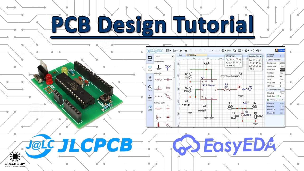
Make Your First Printed Circuit Board
The impedance solver in the Layer Stack Manager enables differential pair solutions as well as single-ended, so you can determine both requirements and use these when routing. After the layer stack is created and any impedance profiles are determined, it's time to set up your circuit board design rules so that you can start placing and routing components. The rules that you do use, especially for manufacturing, should be inline with the specifications and tolerances for your PCB board manufacturer’s equipment. If necessary, you can create new circuit board design rules by following the steps of Altium Designer’s Design Rule Wizard.
One of the key concepts in electronics is the printed circuit board or PCB. It's so fundamental that people often forget to explain what a PCB is. This tutorial will breakdown what makes up a PCB and some of the common terms used in the PCB world. You need to transfer your schematic diagram into a drawing of your printed circuit board. David Haboud joined Altium as a Product Marketing Engineer in 2015.
The Community for Creative Electronics
There’s no denying that some software are better designed and easier to use than others, and it’s often the more professional paid solutions that are the most intuitive. Traces can also be routed automatically using the software’s auto-router. For complicated circuits, it’s generally better to route traces manually, but try the auto-router on simpler designs and see what it comes up with.
Firmware Development Services
Some double layer PCBs have a ground layer, where the entire bottom layer is covered with a copper plane connected to ground. The positive traces are routed on top and connections to ground are made with through holes or vias. Ground layers are good for circuits that are prone to interference, because the large area of copper acts as a shield against electromagnetic fields. Larger circuits can be difficult to design on a single layer PCB because it’s hard to route the traces without intersecting one another. You might need to use two copper layers, with traces routed on both sides of the PCB.
If the printed circuit board shape, dimensions, and layer stackup for your board have already been determined, you can set them now. If you don’t want to do these tasks now, don’t fret, your board shape, size, and layer stackup (see Step 4 below) can be changed later. Schematic information is made available for the PcbDoc by compiling the SchDoc. It is highly recommended that you review and update the Project Options at this point, which are used to create the PcbDoc information. This program offers all the tools you need to create precise PCB layouts efficiently. It offers real-time design insights, including route, placement, coupling, and impedance analysis, to help speed up prototype to production.
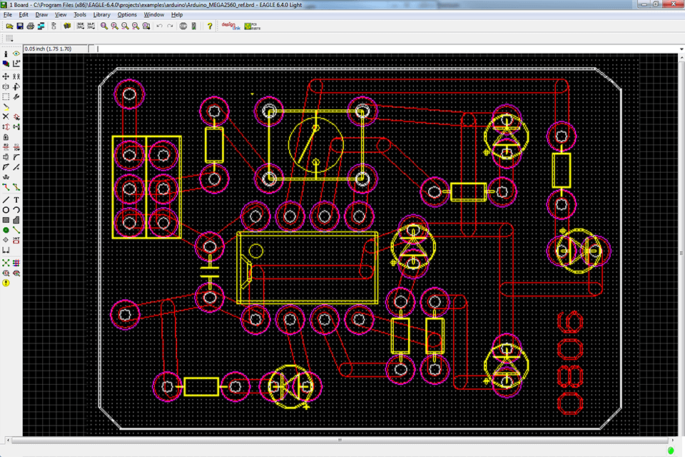
Once your schematic is created and successfully verified, you can transfer your design to a PCB layout, which defines the physical architecture of your board. This may seem simple enough, but each task requires several interdependent steps. Moreover, there are constraints and guidelines that must be followed to ensure your design can actually be manufactured. Create electronic designs from schematic capture to final design documentation and manufacturing files – all in one intuitive interface and unified data model. So, make sure you check that a PCB program offers the features you need before jumping in.
The editor also has an integrated SPICE simulator for testing the viability of circuits before porting them to the real world. Alongside, there’s a robust PCB layout editor with a 3D and Gerber viewer, DRC scripting support, and support for designs from CAD software like EAGLE and the Altium suite. The interactive routing tools allow you to route PCB layouts from any angle at fast speeds, while the Layer Stackup feature helps to reduce noise and improve signal timing even on highly complex circuit boards. As soon as you transfer your schematic data into a new PCB layout, you’ll have to place components around the board. At this point in the design, your goal is to place components to ensure that the design is solvable, meaning it can be routed easily.


No comments:
Post a Comment